Protecting DC-Fed Electronic Equipment
In the past, the biggest problem facing a facilities engineer was the threat of damaging transients created by the operation of highly inductive loads or lightning strikes. Transients are still a problem today, but the proliferation of higher switching frequencies within today's equipment (MHz for power converters and GHz for CPUs), have made electromagnetic interference (EMI) an increasingly troublesome issue.
EMI is one form of emission caused by high switching frequencies. The other is conduction, which occurs when noise is transmitted through electric conductors. In the case of EMI, conductors inside or outside an enclosure act as unintended antennas and transmit electromagnetic waves into the environment. Due to increases in operating frequency, radiation becomes a more prevalent mechanism for EMI. Most of the industry standards limit the upper test frequency for conducted emissions to 30 MHz, while radiated emissions are tested at a higher frequency range.
Suppression methods. Manufacturers and end-users routinely apply a number of measures to prevent EMI from affecting signal lines, especially where the high-frequency signals are present and are an obvious source of EMI. These measures, which include using shielding and twisted pairs, are also used to reduce susceptibility of signal lines to external EMI sources.
However, manufacturers and end-users often overlook power lines when taking EMI prevention steps during the early design stages. A number of factors make power lines important contributors to EMI problems. First, these lines usually provide a large antenna loop area. Second, introduction of inductive components in series with such lines is often very costly, due to the high current those components have to carry. And last, the presence of DC or low-frequency currents causes a saturation of high-frequency inductors.
As is the case with any signal, you can achieve attenuation of EMI noise by connecting either a high serial impedance or low parallel impedance to the signal's source. As previously discussed, implementing a high serial impedance is harder to do than using a low parallel impedance. In fact, connecting a low impedance in parallel with its source is relatively easy to do: Just connect capacitors between the power lines and the system chassis. But it's important to first examine more closely the use of capacitors for shunting high-frequency currents.
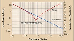
Capacitors and resonant frequency. With a perfect capacitor, you would expect impedance to decrease as frequency increases, as described in the equation Z=1/(2πfC). However, every capacitor has an intrinsic inductance value that, along with its capacitance value, creates a resonant circuit. The self-resonant frequency occurs where the capacitive reactance equals the inductive reactance, as in the equation 1/(2πfC)=2πfL. Fig. 1 shows a graphic representation of this phenomenon.
Further investigation shows that resonant frequency depends on both the lead length (inductance) and the capacitance value. Looking at Fig. 2 on page 22, you can see that different lead lengths (20 mm and 100 mm for a 1µF capacitor) produce different resonance peaks. Fig. 3 on page 24 shows the effect of different capacitor values (0.01µF, 0.1µF, and 1µF) with a 20-mm lead length. The resonant frequency decreases as the capacitance value increases.
The longer the leads, the greater the inductance and lower the self-resonant frequency. Although Fig. 3 represents impedance, you can also use it to represent insertion loss. Therefore, as the frequency increases above the self-resonant point, the capacitor begins to lose its attenuation characteristics. In fact, it starts to function more as an inductor.
Feed-through capacitor in EMI filtering. Based on this insight into capacitors, you can conclude that to create an efficient high-frequency filter, you must minimize parasitic inductance associated with the leads of such a filter. To achieve this goal, you can use a “feed-through capacitor” in place of a regular leaded or SMT device. The feed-through capacitor is constructed in such a way that the current-carrying conductor passes through the capacitor that completely encircles it. While the low-frequency power current is conducted on the spindle, the RF current is shunted through the capacitor to the unit's enclosure.
Due to the design of a feed-through capacitor, the leads are eliminated. The design also allows for the direct connection of the capacitor element to the current-carrying spindle and the grounding plane of the unit. This allows the capacitor to follow its theoretical frequency response. Therefore, as the frequency increases, the impedance of the feed-through capacitor decreases, providing attenuation performance well above 2 GHz.
You can expect some small resonance, but this usually happens due to distributed inductance within the capacitor, which causes a slight deviation from the theoretical performance. A comparison chart of the theoretical vs. actual performance is shown in Fig. 4.
The performance of a feed-through capacitor is driven more by contact resistance between itself and the unit's enclosure. Looking at Fig. 5, you can see the effects of poor grounding as well as the effects on the attenuation performance. Although the graph describes a more complex filter, you can easily see the importance of mounting filters on a clean surface with a good contact. No protective finish (insulating surface) can be on the metal surface, such as paint or zinc. Basically, you need a uniform, low-impedance contact.
One final point to take note of during system design is containment of the radiated energy produced inside of the electronic enclosure. With the ever-increasing operating frequencies of computer and RF equipment, the wavelength of the RF emissions is decreasing (λ=c/f, where λ is wave length, c is the speed of light, and f is frequency), and therefore, even relatively small openings in an enclosure can provide an escape route for unwanted RF emissions.
Armitage is an engineering manager with Schaffner EMC in Edison, N.J. Palagi is senior design engineer, Volfson is principal architecture engineer, and Wojcicki is director of research and development, all with Anderson Power Products in Lowell, Mass.


